
Application-Solution

Wafer Dicing:
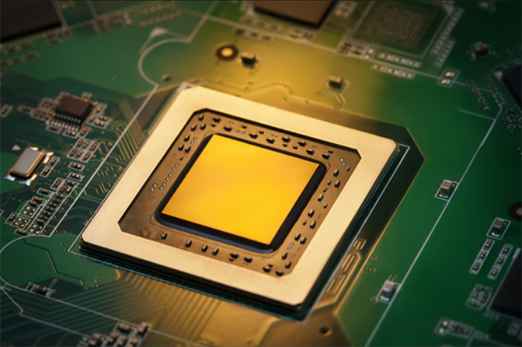
It is a series of semiconductor manufacturing processes to form extremely small circuit structures.
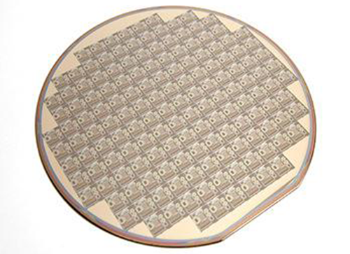
It is then cut, packaged, and tested into chips, which are widely used in various electronic devices. It is also an essential process in the semiconductor chip manufacturing process. Dividing the entire chip wafer into single chips (grains) according to the chip size is called wafer dicing.
In the wafer dicing industry, one is that traditional dicing has the following characteristics:
● Blade scribing directly acts on the surface of the wafer, causing damage inside the crystal, which can easily lead to chipping and damage to the wafer;
● The blade has a certain thickness, resulting in a larger scribing line width;
● The consumables are large and the blade needs to be replaced every half month;
● The environment is polluted, and the silicon powder water after cutting is difficult to handle
-
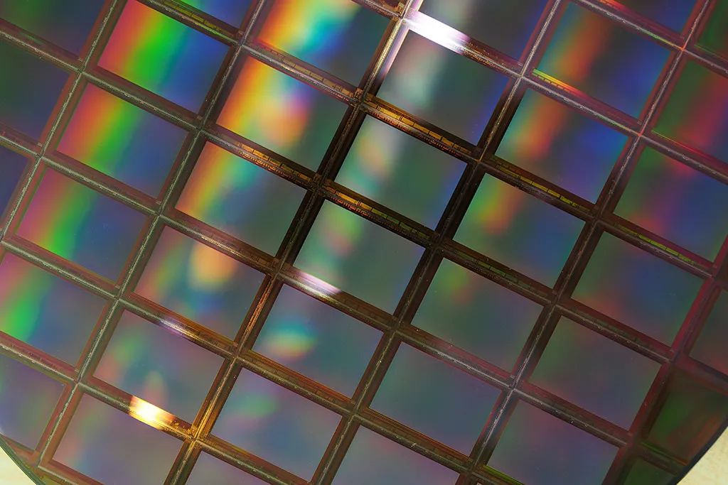
Laser scribing is a non-contact process, which can avoid the above situation.
-
It is used in the cutting of single and double mesa glass passivated diode wafers.
-
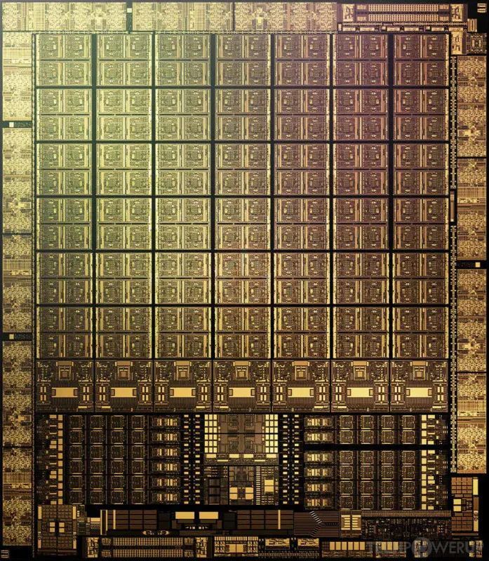
Dividing the entire chip wafer into single chips (grains) according to the chip size is called wafer dicing.
-
The high-beam quality fiber laser used in laser cutting/dicing has little impact on the electrical properties of the chip and can improve the dicing yield.
-
Can work on wafers of different thicknesses, with better compatibility and versatility.
-
Can cut some more complex wafer chips, such as hexagonal die, etc.
-
No deionized water is required, there is no tool wear problem, and it can operate continuously for 24 hours.